
Bias Pinout

Is the bias upper pin connected to the BIAS_INV and the bias lower pin connected to BIAS_DRV or the other way?
https://github.com/OpenBCI/V3_Hardware_Design_Files/blob/master/OpenBCI Cyton Designs/OBCI_V3_32bit-Schematic.jpg
Is the bias upper pin connected to the BIAS_INV and the bias lower pin connected to BIAS_DRV or the other way?
https://github.com/OpenBCI/V3_Hardware_Design_Files/blob/master/OpenBCI Cyton Designs/OBCI_V3_32bit-Schematic.jpg
Comments
No. Both Bias pins are the final 'Bias' / Ground connection.
So there is no difference between the upper and lower Bias pins?
Correct.
Thanks!
In Bias_DRV there's a something called RS IM, what is RS IM?
I see how Bias_DRV connects to the BIAS pins on the cyton, but I don't see Bias_Inv used anywhere, is it necessary?
@bci_sigcraft, I merged your new thread into this existing one.
Please consult the TI ADS1299 for external Bias circuitry recommendations.
On the schematic, BIAS_DRV goes through an RC network, I assume for RF filtering purposes. The two components are R5, a 1 meg resistor, and C16, a 1 nanofarad cap.
If you actually look at the TI data sheet, you can see that BIAS_INV connects all the ADS1299 chips as a BIAS_INV bus. So that all chips cooperate in estimating the common mode noise and derived inverse injection anti-mains voltage.
Other RC pre-filter components are connected on each channel input pin.
https://openbci.com/forum/index.php?p=/discussion/154/front-end-filtering-esd-cmrr-rfi
Hi,
I don't mean in the Bias_INV in the ADS, I mean in the Cyton Schematic I don't see it being connected to anything. Does the Cyton not use Bias_INV?
Compare the Cyton and Daisy schematics. BIAS_INV on both boards are connected, and connected to both ADS1299s.
hi,

I checked Cyton schematic but I could not find any connection to complete feedback loop in bias amplifier. TI recommends this connection from Biasout pin to Biasinv pin over RC circuit as seen on attached figure. (figure 47 in AD1299 datasheet)
According to TI's recommendation, BIAS_DRV net should be connected to BIAS_INV net in the Cyton schematic. However, this is not realized. In the existing case, inverting input of the bias amplifier is left open and this causes amplifier to saturate in negative rail.
Could you please check again?
I don't understand your claim. The Cyton's have been working fine for many years. It's remotely possible that the schematic does not completely reflect the PC board layout, but very unlikely.
The diagram you show above is a TEST configuration, not intended for normal operation.
William
William,


Please check Cyton schematic. According to it, BIAS_DRV and BIAS_INV nets are not connected to each other. I measured high impedance between ADS1299 pin 61 and related pin of resistor array R6. This measurement complies with the schematic.
This means there is no negative feedback for internal bias amplifier of ads1299. As you know, to adjust gain, amplifiers should be supplied with negative feedback. To compensate common voltage utilizing bias output, following loop is recommended.
winter1983
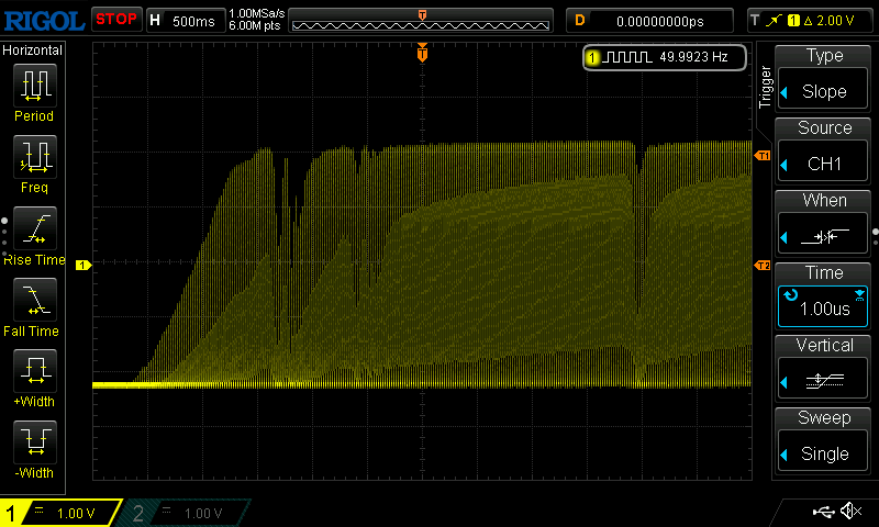
Below is the what I measured at Bias output
Please notice that; this situation does not completely destructs the functionality of the card but deterioriertes common mode rejection capability so Cyton cards continue to work many years.
Regards,
Eray
https://arxiv.org/pdf/1606.02438.pdf
OK. Go on as it is